
Summary
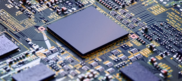
A new design center providing scalable ASIC, FPGA, and SoC design services (analog, digital, mixed-signal) for global chipmakers, accelerating time-to-market and cementing India’s role in advanced semiconductor design innovation. A “Scalable Semiconductor Design Center of Excellence” directly addresses the lack of scalable design expertise in India by offering comprehensive ASIC, FPGA, and SoC design services across analog, digital, and mixed-signal domains. This center provides global chipmakers with readily available, high-quality, and scalable design capacity, significantly reducing time-to-market for advanced semiconductor development and positioning India as a key hub for design innovation.
Problem
Lack of scalable design expertise for advanced semiconductor development
Impact
Supports global chipmakers with design innovation from India
Partners
Technology Providers , FPGA vendors , Mahindra , Raymond